

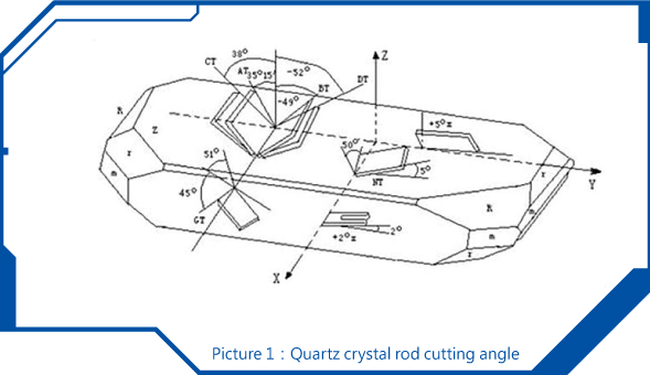
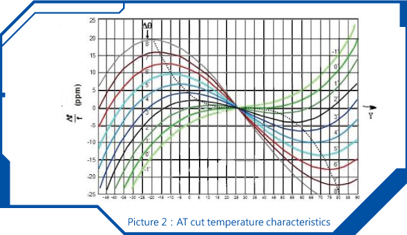
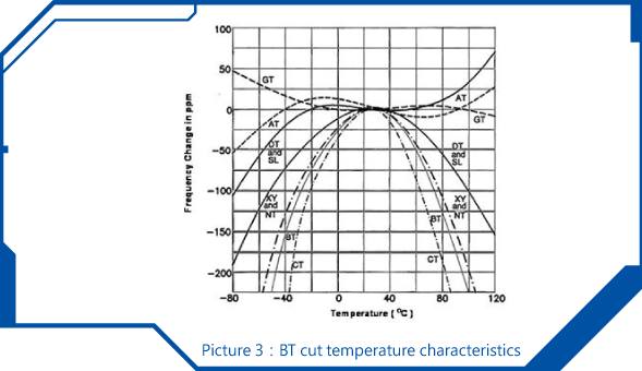
The electrical performance of the product varies based on different temperature. The various quartz cuts cause different electrical specification as well. Usually, the cutting of a quartz wafer to a certain orientation (angle) of the axis of the crystal rod is called the cutting type of the quartz wafer (see picture 1). AT cut is 35 degrees and BT cut is 49 degrees. Both are suitable for the frequency range from MHz to hundreds MHz. In addition, there are different temperature and frequency curve between AT cut and BT cut (see picture 2.3). The temperature frequency of BT cut has higher deviation. The temperature frequency of AT cut is relatively more stable. Therefore, AT cut is widely applied to quartz wafer.
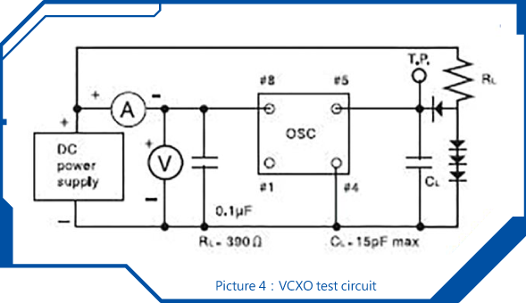
A VCXO is a voltage-controlled crystal oscillator whose output frequency can be controlled by an additional control voltage. A change of the control voltage can change the capacitance value of the capacitor diode (= varicap) which is part of the quartz oscillator circuit. A change of the capacitance value causes a change of the total load capacitance of the quartz oscillator circuit that leads to a different output frequency of the quartz oscillator. So by changing the control voltage you can adjust the quartz oscillator output frequency by a small amount of ppm. The adjustment range can be up to ±200 ppm or even larger. The commonly used supply voltages are 1.8 V, 2.5 V, 3.0 V, 3.3 V and 5 V, of which 3.3 V is the most often used voltage.
A VCXO is featured with a voltage control function and is used in the output frequency circuit for data signal acquisition, jitter attenuation or frequency synthesizing. The current consumption is not higher than 2 mA and it starts quickly and works under low voltage, low drive level and low current consumption and the characteristics of the product are:
1. Wide frequency modulation range
2. Good frequency tolerance and high frequency stability
3. Low jitter or low phase noise characteristics
Note: The jitter generated in the VCXO output signal can have negative effects on the circuit design of other affected circuit areas. Usually the smaller the jitter of a VCXO the better
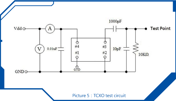
TCXO is the abbreviation of “temperature compensated xtal oscillator”. TCXO is a crystal oscillator with a temperature compensation circuit that reduces frequency changes caused by changes over the operating temperature. It is an active component and able to maintain a frequency stability in the range of ±0.5 ppm to ±5 ppm over its entire operating temperature range.
Due to the higher frequency stability, the compact size and the reduced power consumption a TCXO is typically used as reference clock in mobile phones of mobile communications systems. The required frequency stability of a mobile phone typically lies between ±0.1 and ±2.5 ppm (e.g. for -30 °C to +75 °C as operating temperature range). But as tighter frequency stabilities lead to increasing component cost, the frequency stability of the oscillator shall not be specified tighter than necessary. So often a frequency stability of ±1.5 to ±2.5 ppm over the operating temperature range is already sufficient for the application and saves cost.
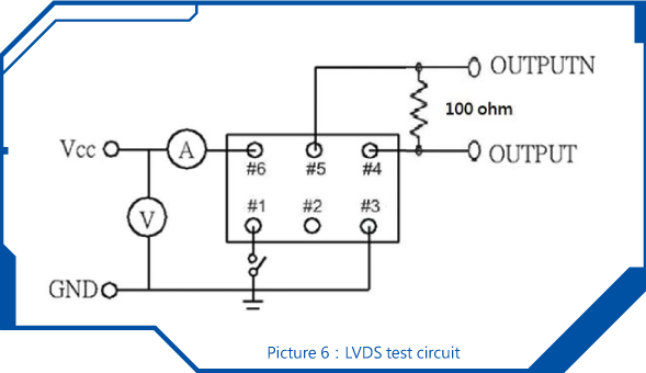
LVDS - Low-Voltage Differential Signaling is a differential signaling system, meaning that it transmits information as the difference between the voltages on a pair of wires; the two wire voltages are compared at the receiver with a terminal resistance (100 Ohm) to create a differential voltage of 350 mV.
This differential voltage signal is suitable for high speed data transmission applications, providing better noise immunity for wired data transmission and a small voltage swing to reduce power consumption on the line.
Advantages of LVDS output:
1. Less susceptible to noise interference
2. Lower EMI emissions compared to CMOS/TTL
3. lower voltage fluctuations (typically 350 mV) and lower power consumption compared to LVPECL outputs
Disadvantages of LVDS output:
1. Reduced jitter performance compared to LVPECL
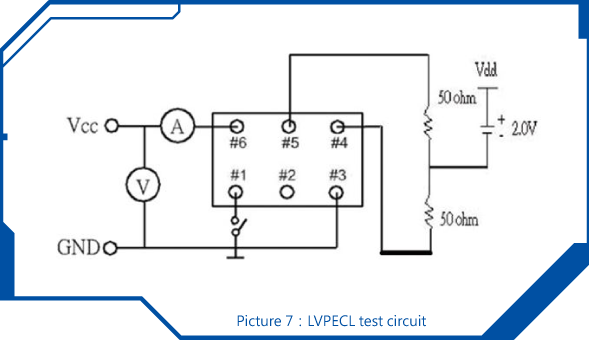
LVPECL - Low Voltage Positive Emitter-Couple Logic. Compared with the general CMOS signal output form, the LVPECL signal has a shorter rise and fall time and is not so sensitive to noise interference, which makes it more suitable for applications with higher noise sensitivity (time-pulse and signal transmission).
Advantages of LVPECL output:
1. Able to drive long transmission lines
2. Ideal for high speed circuit applications
3. Good jitter characteristics due to large voltage swing of differential output
Disadvantages of LVPECL output:
1. Not compatible with 1.8 V power supply
2. Larger power consumption compared with single-ended output
